General Description
The Evaluation Board demonstrates the RT1735’s capability to be designed for Type-C interface overvoltage protection IC. The RT1735 protects the high voltage shorted to VBUS to adjacent pins of CC/SBU up to 28V due to USB Power Delivery (PD), which allows VBUS from 3.3 to 28V sourcing.
The RT1735 is integrated with the protection against ESDs as per IEC61000-4-2 standards, with contact discharge of ±8kV on CON_CC1/CON_CC2, D1/D2 and CON_SBU1/ CON_SBU2.
Performance Specification Summary
Table 1 shows the summary of the RT1735 Evaluation Board performance specificiaiton. The ambient temperature is 25°C.
Table 1. RT1735 Evaluation Board Performance Specification Summary
|
Specification
|
Test Conditions
|
Min
|
Typ
|
Max
|
Unit
|
|
VDD Input Voltage Range
|
|
2.5
|
--
|
5.5
|
V
|
|
CC1/2 Swtich Current
|
|
-1.25
|
--
|
1.25
|
A
|
|
SBU1/2 Swtich Current
|
|
-100
|
--
|
100
|
mA
|
|
CON_CC1/2 & CON_SBU1/2 & D1/2
IEC 61000-4-2 Contact Discharge
|
|
-8k
|
--
|
8k
|
V
|
|
CON_CC1/2 & CON_SBU1/2 & D1/
IEC 61000-4-2 Air Discharge
|
|
-15k
|
--
|
15k
|
V
|
|
CON_CC1/2 & CON_SBU1/2 Short to VBUS
|
|
--
|
--
|
28
|
V
|
Power-up Procedure
Suggestion Required Equipments
- RT1735 Evaluation Board
- DC power supply capable of at least 28V and 5A
- Oscilloscope
Proper measurement equipment setup and follow the procedure below.
1) With power off, connect the input power supply to the VDD and GND pins.
2) Turn on the power supply at VDD. Make sure that the CC/SBU Switch turn on.
3) Once the Switch is turn, test OVP threshold and OVP & ESD performance.
Detailed Description of Hardware
Headers Description and Placement
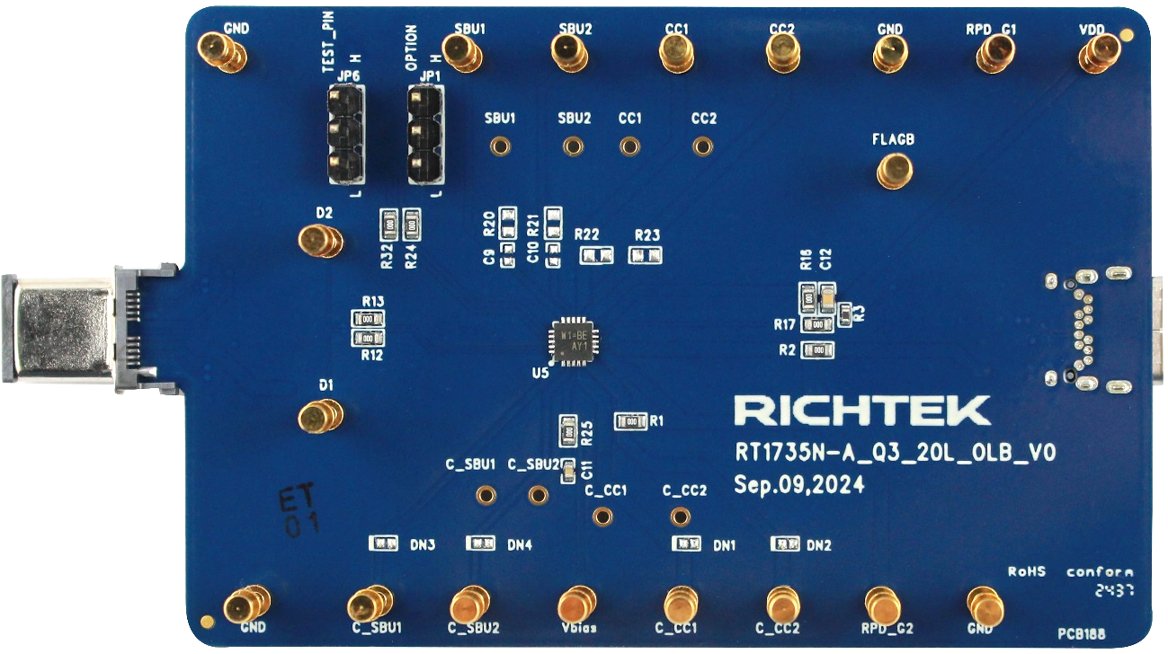
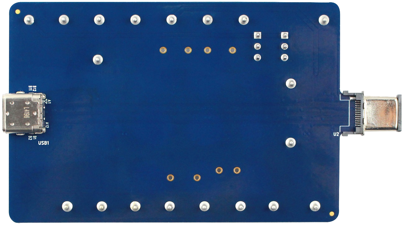
Carefully inspect all the components used in the EVB according to the following Bill of Materials table, and then make sure all the components are undamaged and correctly installed. If there is any missing or damaged component, which may occur during transportation, please contact our distributors or e-mail us at evb_service@richtek.com.
Test Points
The EVB is provided with the test points and pin names listed in the table below.
|
Test Point/
Pin Name
|
Function
|
|
VDD
|
Input voltage.
|
|
FLAGB
|
Open-drain output cautioning fault condition.
|
|
VBIAS
|
VBIAS pin connect capacitor for ESD protection. Put a 0.1µF capacitor on this pin to ground.
|
|
GND
|
Ground.
|
|
CON_CC1
|
Type-C connector side CC1 switch. Connect the CC1 pin of the USB Type-C connector.
|
|
CON_CC2
|
Type-C connector side CC2 switch. Connect the CC2 pin of the USB Type-C connector.
|
|
CON_SBU1
|
Type-C connector side SBU1 switch. Connect the SBU1 pin of the USB Type-C connector.
|
|
CON_SBU2
|
Type-C connector side SBU2 switch. Connect the SBU2 pin of the USB Type-C connector.
|
|
RPD_G1
|
If dead battery resistors are required, short pin to CON_CC1. If dead battery resistors are not required, short pin to GND.
|
|
RPD_G2
|
If dead battery resistors are required, short pin to CON_CC2. If dead battery resistors are not required, short pin to GND.
|
|
CC1
|
System side of the CC1 switch. Connect to the CC pin of the CC/PD controller.
|
|
CC2
|
System side of the CC2 switch. Connect to the CC pin of the CC/PD controller.
|
|
SBU1
|
System side of the SBU1 switch. Connect to the SBU pin of the SBU MUX.
|
|
SBU2
|
System side of the SBU2 switch. Connect to the SBU pin of the SBU MUX.
|
|
D1
|
USB2.0 IEC ESD protection. Connect to the USB2.0 pins of the USB Type-C connector.
|
|
D2
|
USB2.0 IEC ESD protection. Connect to the USB2.0 pins of the USB Type-C connector.
|
Bill of Materials
|
Reference
|
Count
|
Part Number
|
Value
|
Description
|
Package
|
Manufacturer
|
|
U5
|
1
|
RT1735N-A
|
RT1735N-A
|
OVP Switch
|
WQFN-20L 3x3
|
RICHTEK
|
|
U2
|
1
|
121U-AC2C-0XXT
|
USB TYPE C Plug Conntecter
|
USB TYPE C Plug Conntecter
|
12.6x10.6x4.1 mm
|
JEM
|
|
USB1
|
1
|
C-NBR2L-00-00
|
USB TYPE-C Female Conntecter
|
USB TYPE-C Female Conntecter
|
9.24x9.1mm
|
ADVANCED-CONNECTEK
|
|
C9, C10, C11
|
3
|
0402B104K500CT
|
100nF
|
Capacitor, Ceramic, 50V, X7R
|
0402
|
WALSIN
|
|
C12
|
1
|
0603X105K250CT
|
1µF
|
Capacitor, Ceramic, 25V, X5R
|
0603
|
WALSIN
|
|
R1, R2, R12, R13, R16, R17, R24, R25, R32
|
9
|
WR06X000 PTL
|
0Ω
|
Resistor, Chip, 1/10W, 1%
|
0603
|
WALSIN
|
|
R3
|
1
|
RTT021003FTH
|
100kΩ
|
Resistor, Chip, 1/16W, 1%
|
0402
|
RALEC
|
|
R20, R21
|
2
|
WR06X30R1FTL
|
30.1Ω
|
Resistor, Chip, 1/10W, 1%
|
0603
|
WALSIN
|
|
R22, R23
|
2
|
WR06X30R0FTL
|
30Ω
|
Resistor, Chip, 1/10W, 1%
|
0603
|
WALSIN
|
Typical Applications
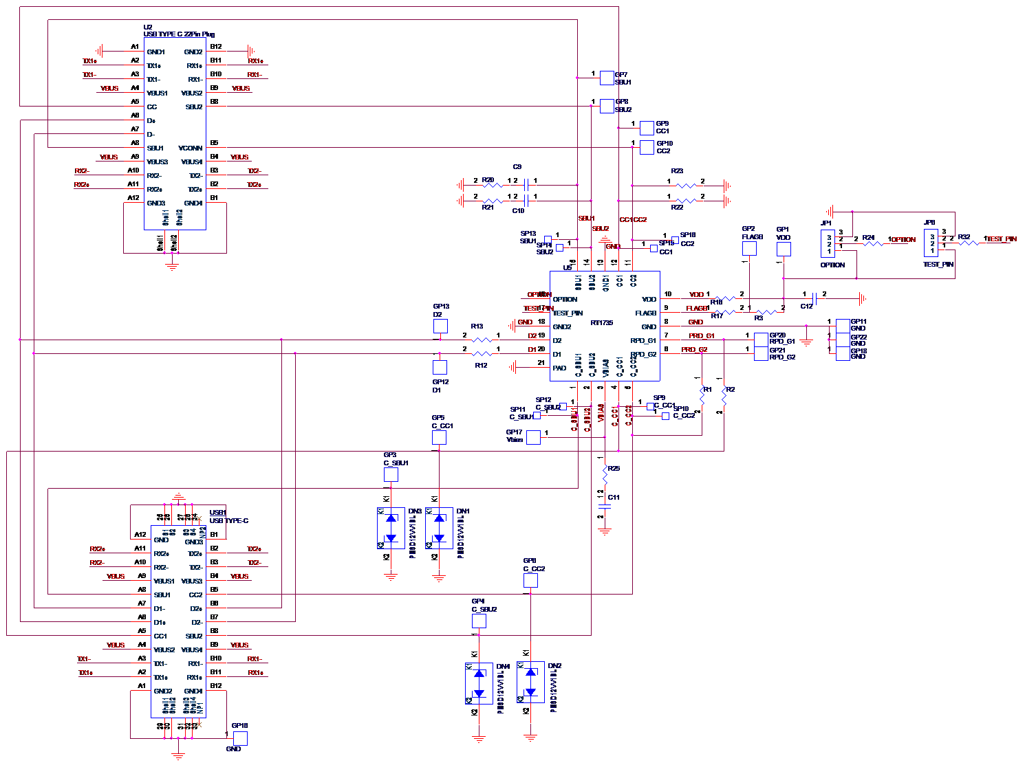
EVB Schematic Diagram
Measurement Result
|
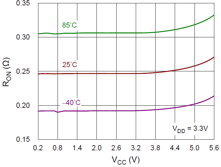
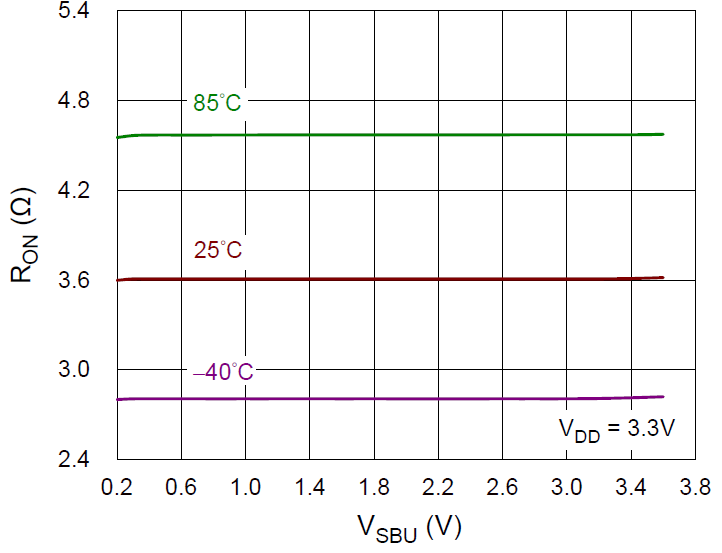
CC Switch Ron
|
SBU Switch Ron
|
|
|
|
|
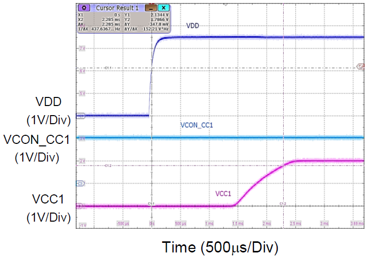
CC Switch Turn on Timing
|
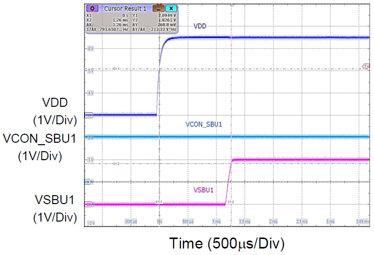
SBU Switch Turn on Timing
|
|
|
|
|
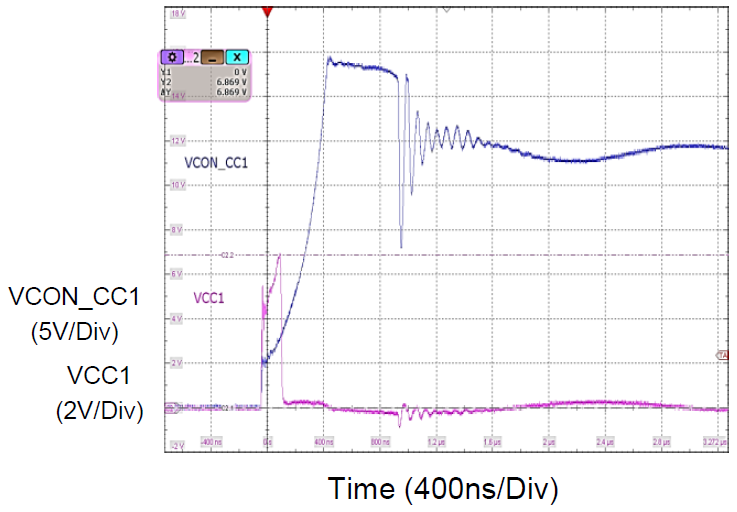
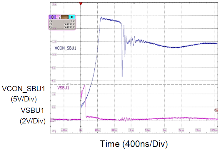
CC Clamp Voltage on System Side
|
SBU Clamp Voltage on System Side
|
|
|
|
Evaluation Board Layout
Figure 1 to Figure 8 are RT1735 Evaluation Board layout. This board size is 82mm x 51mm and is constructed on eight-layer PCB, outer layers with 1 oz. Cu and inner layers with 1 oz. Cu.
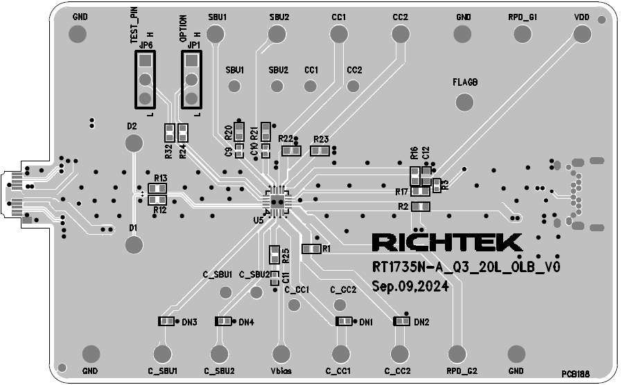
Figure 1. Top View (1st layer)
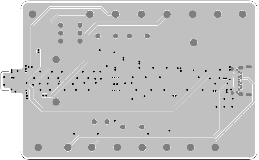
Figure 2. PCB Layout—Inner Side (2nd Layer)
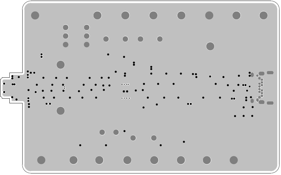
Figure 3. PCB Layout—Inner Side (3rd Layer)
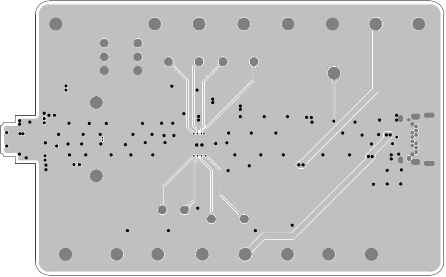
Figure 4. PCB Layout—Inner Side (4th Layer)
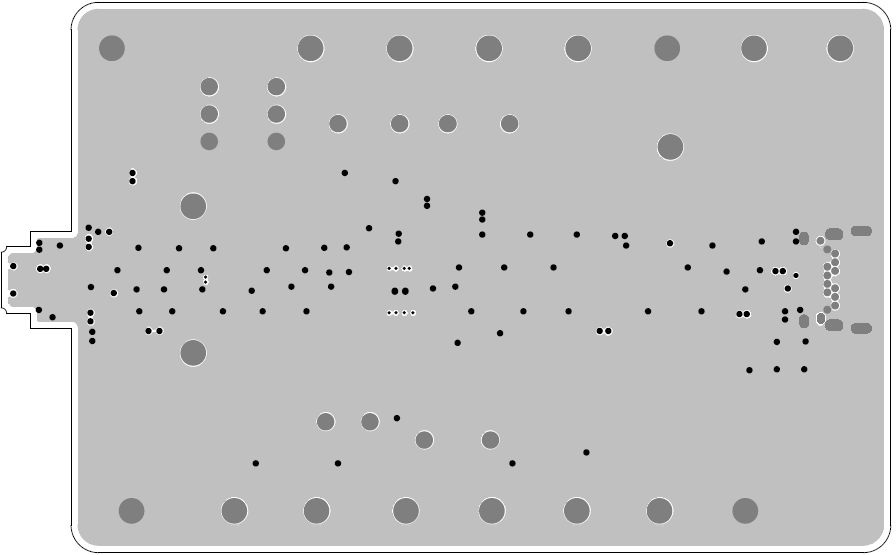
Figure 5. PCB Layout—Inner Side (5th Layer)
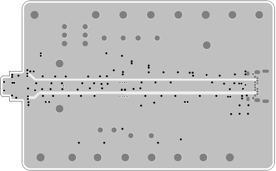
Figure 6. PCB Layout—Inner Side (6th Layer)
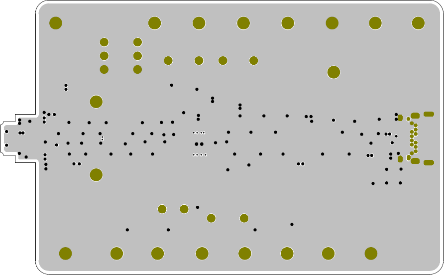
Figure 7. PCB Layout—Inner Side (7th Layer)
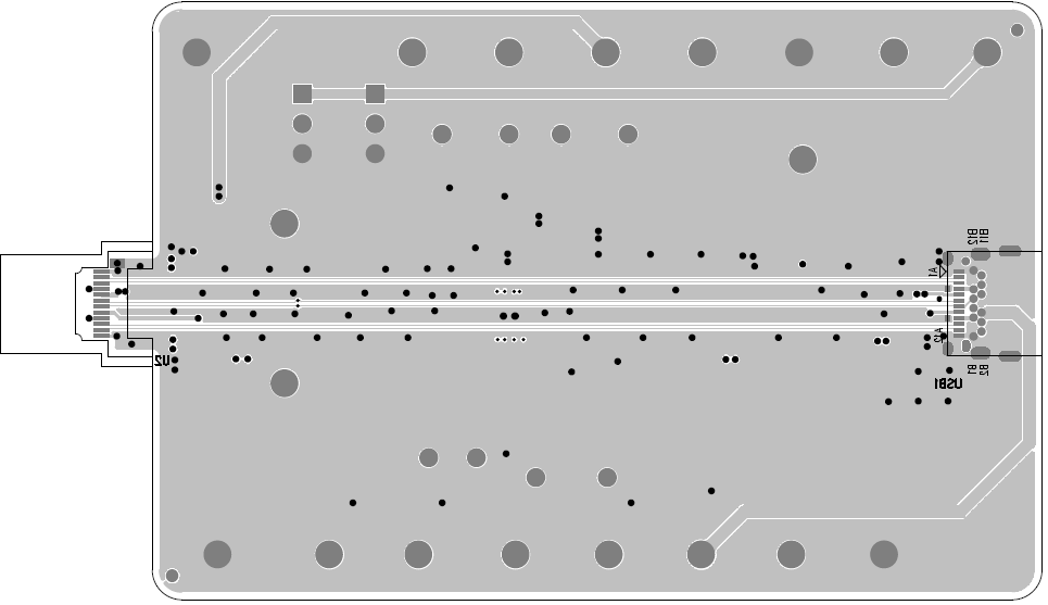
Figure 8. Bottom View (8th Layer)